Reverse breakdown of Junction diode
The amount of reverse bias voltage at which current passing through a junction diode increases abruptly is called reverse breakdown voltage, and the process is called breakdown of the junction diode.
The breakdown of the junction diode doesn’t mean that the diode has been damaged physically; only that the barrier breaks and current increases suddenly while the breakdown of the junction diode.
There are two breakdown processes in pn-junction diode,
- Zener breakdown
- Avalanche breakdown
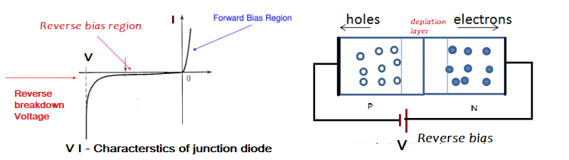
Table of Contents
Zener Breakdown of pn-junction Diodes
Zener breakdown occurs in heavily doped pn-junction diodes. This breakdown in the junction diode is due to band to band tunneling. When a large reverse bias voltage is applied across a pn-junction diode, it sets up a high electric field (as the width of the depletion layer is small, V = E/d), which enables tunnelling of electrons from the valence to the conduction band of the semiconductor. Due to this, there are a large number of free minority carriers in the conduction band of the semiconductor, which suddenly increases the reverse current through the junction diode.
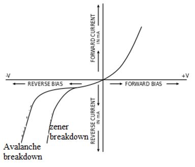
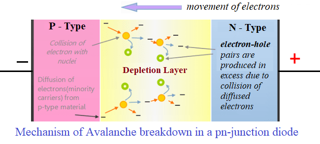
Avalanche breakdown
Avalanche breakdown occurs in lightly doped junction diodes. Here width of the depletion layer is large, so the applied electric field is not enough to produce Zener breakdown. If the applied voltage is increased (more than the Zener breakdown voltage), it breaks the covalent bonds between atoms in the semiconductor and new electron-hole pairs are generated. Newly generated electron-hole pairs are accelerated by the applied electric field and move with high energy. These highly energetic charge carriers collide with more bonded electrons and an avalanche of charge carriers is produced, due to which current increases sharply.
Important questions from the Topic
What is Zener breakdown of a junction diode?
Ans: Zener breakdown is a type of reverse breakdown that occurs in a junction diode with a heavily doped p-n junction. It is characterized by a sudden increase in current flow at a specific reverse voltage, called the Zener voltage.
What is the difference between Zener breakdown and avalanche breakdown?
Ans: Zener breakdown occurs in heavily doped junctions, where the electric field is strong enough to strip electrons from the covalent bonds in the depletion region, creating electron-hole pairs and allowing current to flow. Avalanche breakdown occurs in lightly doped junctions, where the electric field is not strong enough to create electron-hole pairs, but instead accelerates free electrons to high energies that can create additional electron-hole pairs through collisions with the atoms in the semiconductor material.
What is the Zener voltage?
Ans: The Zener voltage is the specific reverse voltage at which Zener breakdown occurs in a diode. It is a characteristic of the diode and is determined by the doping concentration of the p-n junction. Zener diodes are specifically designed to have a precise Zener voltage.
How is Zener breakdown used in electronic circuits?
Ans: Zener diodes are commonly used as voltage regulators in electronic circuits. They provide a stable reference voltage that remains constant even if the input voltage varies. Zener diodes can also be used as protection devices in circuits that may be subject to voltage spikes or transients.
Can a junction diode be damaged by Zener breakdown?
Ans: If a junction diode is subjected to a reverse voltage that exceeds its maximum allowable rating, it may be damaged or destroyed by Zener breakdown. Therefore, it is important to select the appropriate diode for the application and to operate it within its specified voltage range.
Is Zener breakdown a reversible process?
Ans: In general, once a junction diode has undergone Zener breakdown, its characteristics are permanently altered. However, Zener diodes are specifically designed to operate in Zener breakdown mode, and can be used reliably over a long period of time if operated within their specified parameters
Q: What is avalanche breakdown?
Answer: Avalanche breakdown is a phenomenon that occurs in semiconductor devices, particularly diodes, when a high reverse voltage is applied to them. It refers to the rapid increase in current flow due to the multiplication of charge carriers through impact ionization.
Q: How does avalanche breakdown happen?
Answer: When a high reverse voltage is applied to a semiconductor device, the electric field across the depletion region becomes strong enough to cause electrons and holes to gain enough energy through collisions with atoms to free additional charge carriers. These newly generated charge carriers can then collide with other atoms, creating more charge carriers in a chain reaction, leading to a rapid increase in current flow.
Q: What is the significance of avalanche breakdown?
Answer: It has both positive and negative implications. In some cases, avalanche breakdown is intentionally utilized in devices such as avalanche diodes and Zener diodes, where it allows them to operate as voltage regulators or voltage references. On the other hand, avalanche breakdown can also be an undesirable effect in other semiconductor devices, as it can lead to device failure if not properly controlled or protected.
Q: How is avalanche breakdown different from Zener breakdown?
Answer: Avalanche breakdown and Zener breakdown are two distinct mechanisms of breakdown in diodes. The primary difference lies in the mechanism of charge carrier generation. In avalanche breakdown, charge carriers gain energy through impact ionization, while in Zener breakdown, charge carriers gain energy through the tunneling effect across the depletion region.
Q: What factors influence avalanche breakdown?
Answer: It is influenced by several factors, including the doping concentration in the semiconductor material, the thickness of the depletion region, and the temperature. Higher doping concentrations and narrower depletion regions generally increase the likelihood of avalanche breakdown. Additionally, elevated temperatures can lower the breakdown voltage and increase the rate of carrier multiplication.
Q: Can avalanche breakdown damage semiconductor devices?
Answer: Yes, if not properly managed, avalanche breakdown can lead to device failure or damage. When excessive current flows during avalanche breakdown, it can generate heat and cause localized hotspots, leading to thermal runaway and ultimately damaging the device. It is important to implement appropriate protection measures, such as current limiting or thermal management, to prevent damage in high-power applications.
Q: How is avalanche breakdown different from thermal breakdown?
Answer: Avalanche breakdown is primarily caused by the impact ionization of charge carriers, whereas thermal breakdown occurs due to excessive heat generation in a semiconductor device. While avalanche breakdown can be triggered by a high voltage, thermal breakdown is related to the dissipation of power and the inability to adequately dissipate heat.
Q: Can avalanche breakdown occur in materials other than semiconductors?
Answer : It is predominantly observed in semiconductor materials due to their specific energy band structure and the presence of a depletion region. Other materials, such as insulators and conductors, generally do not exhibit avalanche breakdown as their electronic properties differ significantly from semiconductors.
Q: What is a breakdown of a junction diode?
Answer : The breakdown of a junction diode refers to a phenomenon where the diode loses its ability to regulate current flow and experiences a sudden increase in current when a certain voltage threshold is reached. This breakdown can occur in two different ways: Zener and avalanche .
Q: What is Zener breakdown?
Answer : Zener breakdown occurs in a heavily doped semiconductor diode, known as a Zener diode, operating in the reverse-biased condition. When the reverse voltage across the diode exceeds the Zener voltage (also called the breakdown voltage), a significant amount of current starts to flow in the reverse direction. The Zener breakdown is a controlled breakdown, and the voltage remains nearly constant even as the current increases.
Q: What are the causes of breakdown in junction diodes?
Answer : The breakdown in junction diodes can be caused by several factors. In Zener breakdown, the heavily doped regions of a Zener diode allow for a narrow depletion region, enabling a controlled breakdown to occur. In avalanche breakdown, the high reverse voltage creates a strong electric field across the lightly doped region, resulting in the ionization of atoms and the subsequent breakdown.
Q: What are the applications of Zener breakdown?
Answer : Zener breakdown is intentionally utilized in Zener diodes, which are designed to operate in the breakdown region. Zener diodes are widely used as voltage regulators in various electronic circuits. They can maintain a nearly constant voltage across their terminals, even when the current varies significantly. This property makes them useful for voltage stabilization and protection against voltage spikes.
Q: What are the applications of avalanche breakdown?
Answer : However, avalanche breakdown is utilized in some specialized devices such as avalanche diodes, which are designed to operate in the breakdown region. It is used in applications such as surge protection, voltage clamping, and high voltage measurement circuits.
Q: What are the consequences of exceeding the breakdown voltage in a diode?
Answer : Exceeding the breakdown voltage in a diode can lead to significant current flow and potential damage to the diode or the circuit it is connected to. In normal operating conditions, diodes are designed to operate within a specific voltage range, and exceeding the breakdown voltage can cause a breakdown in the diode’s regulation function, leading to unpredictable behavior and potential circuit failure.
Q: How can breakdown in junction diodes be prevented?
Answer : Breakdown in junction diodes can be prevented by using diodes with appropriate voltage ratings for a given application. Selecting diodes with breakdown voltages that exceed the expected operating voltage is essential.
What is reverse breakdown of a junction diode?
Ans: The reverse breakdown of a junction diode is a phenomenon in which a large reverse voltage applied to the diode causes a sudden increase in current flow through the device. This is also known as “reverse breakdown voltage” or “Zener breakdown”.
How does reverse breakdown occur in a junction diode?
Ans: In a junction diode, a depletion region exists between the p-type and n-type semiconductor layers. When a reverse voltage is applied to the diode, the depletion region widens and the electric field across it increases. At a certain voltage, called the breakdown voltage, the electric field becomes strong enough to ionize the atoms in the depletion region and cause a flow of current through the diode.
What is the difference between Zener breakdown and avalanche breakdown?
Ans: Zener breakdown occurs in heavily doped junctions, where the electric field is strong enough to strip electrons from the covalent bonds in the depletion region, creating electron-hole pairs and allowing current to flow. Avalanche breakdown occurs in lightly doped junctions, where the electric field is not strong enough to create electron-hole pairs, but instead accelerates free electrons to high energies that can create additional electron-hole pairs through collisions with the atoms in the semiconductor material.
What are some practical applications of reverse breakdown in junction diodes?
Ans: Reverse breakdown is used in many electronic circuits, such as voltage regulators and voltage reference sources. Zener diodes, which are designed specifically for reverse breakdown, are commonly used to stabilize voltage levels in electronic devices. Avalanche diodes are used in high-voltage applications, such as power supplies and surge protection circuits.
Is reverse breakdown of a junction diode a reversible process?
Ans: In general, once a junction diode has undergone reverse breakdown, its characteristics are permanently altered. However, some diodes are designed to operate in reverse breakdown mode (called zener diode), and can be used reliably over a long period of time if operated within their specified parameters.
What types of dopants are commonly used in semiconductor materials, and how do they affect the material’s properties?
Common dopants used in semiconductor materials include boron, phosphorus, arsenic, and antimony belongs to 13th and 15th group elements of periodic table. These dopants can donate or accept electrons, which affects the material’s electrical conductivity, and they can also modify its optical and thermal properties.
How does the doping concentration of a semiconductor material affect its electrical conductivity?
The doping concentration of a semiconductor material can significantly affect its electrical conductivity. Higher doping concentrations generally lead to higher conductivity, since more charge carriers are present in the material.
What is a semiconductor, and what does its energy band diagram look like?
Ans: A semiconductor is a material that has an intermediate level of electrical conductivity between a conductor and an insulator. Its energy band diagram shows a small energy gap (bandgap) between the valence and conduction bands. This gap can be overcome by adding energy, such as heat or light, to the material.
What is an insulator, and what does its energy band diagram look like?
Ans: An insulator is a material that has a high resistance to the flow of electrical current. Its energy band diagram shows a large energy gap between the valence and conduction bands, which means that it requires a significant amount of energy to move an electron from the valence band to the conduction band.
What is a rectifier?
A rectifier is an electronic device that converts alternating current (AC) to direct current (DC). It does this by allowing current to flow in only one direction through a circuit, typically using a diode or a series of diodes.
Zener Breakdown of pn-Junction Diodes, Zener Breakdown of pn-Junction Diodes, Zener Breakdown of pn-Junction Diodes, Zener Breakdown of pn-Junction Diodes, Zener Breakdown of pn-Junction Diodes, Zener Breakdown of pn-Junction Diodes, Zener Breakdown of pn-Junction Diodes, Zener Breakdown of pn-Junction Diodes, Zener Breakdown of pn-Junction Diodes, Zener Breakdown of pn-Junction Diodes
Zener Breakdown of pn-Junction Diodes, Zener Breakdown of pn-Junction Diodes, Zener Breakdown of pn-Junction Diodes, Zener Breakdown of pn-Junction Diodes, Zener Breakdown of pn-Junction Diodes, Zener Breakdown of pn-Junction Diodes, Zener Breakdown of pn-Junction Diodes, Zener Breakdown of pn-Junction Diodes, Zener Breakdown of pn-Junction Diodes, Zener Breakdown of pn-Junction Diodes
Zener Breakdown of pn-Junction Diodes, Zener Breakdown of pn-Junction Diodes, Zener Breakdown of pn-Junction Diodes, Zener Breakdown of pn-Junction Diodes, Zener Breakdown of pn-Junction Diodes, Zener Breakdown of pn-Junction Diodes, Zener Breakdown of pn-Junction Diodes, Zener Breakdown of pn-Junction Diodes, Zener Breakdown of pn-Junction Diodes, Zener Breakdown of pn-Junction Diodes
Thank you for providing me with these article examples. May I ask you a question?
Thank you for your valuable feedback 😊. YES, PLEASE ASK.
The articles you write help me a lot and I like the topic
Thank you for your valuable feedback 😊.