Table of Contents
pn Junction Formation
pn Junction Formation : A pn-junction can be formed by growing p and n-type impurities onto a block of pure Si/Ge crystal or joining p and n-type wafers to each other by melting at the junction.
Two important processes that occur during the formation of a p-n junction are (i) diffusion and (ii) drift.
(i) diffusion:
In an n-type semiconductor, electron concentration is greater than hole concentration, whereas in a p-type semiconductor, hole concentration is greater than electron concentration. During the formation of p-n junction, due to the concentration gradient across p-sides and n-sides, holes diffuse from p-side to n-side (p→n) and electrons diffuse from n-side to p-side (n→ p). This motion of charge carriers gives rise to a current called diffusion current.
When an electron diffuses from n → p, it leaves behind an ionized donor (positive charge) on the n-side, which is immobile as it is bonded to the surrounding atoms. As the electrons continue to diffuse from n → p, a layer of positive charge (or positive space-charge region) on the n-side of the junction is developed.
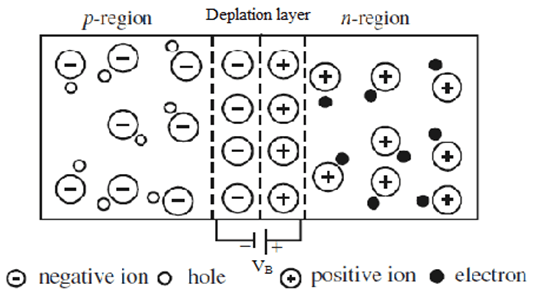
Similarly, when a hole diffuses from p → n due to the concentration gradient, it leaves behind an ionised acceptor (negative charge) which is also immobile. As the holes continue to diffuse, a layer of negative charge (or negative space-charge region) on the p-side of the junction is developed. This space-charge region on either side of the junction is depleted of free charge carriers and is known as the depletion layer.
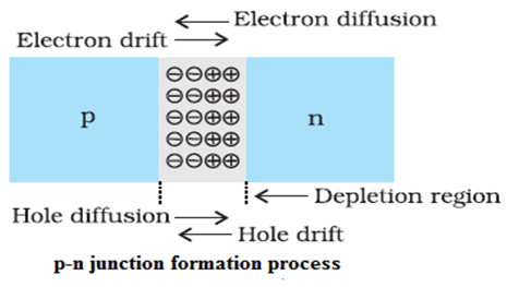
(ii) drift:
Due to the positive space charge region on the n-side of the junction and the negative space charge region on the p-side of the junction, an electric field is developed. Due to this electric field, an electron from the p-side of the junction moves to n-side and a hole from the n-side of the junction moves to the p-side. The motion of charge carriers due to the electric field across the depletion layer is called drift. Here, drifting of charge carriers produces a current called drift current, which is opposite in direction to the diffusion current.
Initially, diffusion current is large and drift current is small. As the diffusion process continues, drift current increases until the diffusion current equals the drift current and now a p-n junction is formed. In a p-n junction under equilibrium, there is no net current.
pn Junction Formation
Important questions from pn Junction Formation
What are the factors influencing the thickness of the depletion layer?
The width of the depletion layer is determined by
(i) The type of biasing: In the forward bias of a pn-junction diode, the thickness of the depletion layer is less in comparison with the reverse bias.
(ii) The extent of doping: The greater the extent of doping, the narrower the depletion layer. More charge carriers will be available at higher dopant concentrations, so they have to move less distance to form a covalent bond, reducing the thickness of the depletion layer.
What is the order of thickness of depletion layer?
The thickness of depletion region is of the order of one-tenth of a micro-metre.
What is a pn-junction?
A pn-junction is the interface between a p-type and an n-type semiconductor. It is formed by doping one region of a semiconductor with impurities that create an excess of free electrons (n-type) and another region with impurities that create a deficiency of free electrons (p-type).
How is a pn-junction formed?
A pn-junction is formed by a process called doping, where impurities are intentionally introduced into a semiconductor crystal. In the case of a pn-junction, the p-type and n-type regions are formed by doping the semiconductor with impurities that either donate (n-type) or accept (p-type) free electrons.
What happens at the junction of a pn-junction?
At the junction of a pn-junction, the n-type and p-type regions come into contact, creating a depletion region. This region is depleted of free charge carriers (electrons and holes) due to the recombination of the majority carriers from each side.
What is the role of the depletion region in a pn-junction?
The depletion region in a pn-junction acts as a barrier to the flow of electric current, creating a potential difference across the junction. This potential difference is called the built-in potential and is a key feature of the pn-junction, as it allows the device to act as a rectifier, converting AC to DC.
(pn Junction Formation)
How does the applied voltage affect a pn-junction?
When a voltage is applied to a pn-junction in the forward bias direction, it reduces the potential barrier and allows current to flow through the junction. In the reverse bias direction, the potential barrier increases, preventing current flow except for a very small reverse current due to minority carriers.
What is the role of the bandgap in pn Junction Formation ?
The bandgap is the energy difference between the valence band and the conduction band of a semiconductor. In pn-junction formation, the bandgap plays a critical role in determining the behavior of the device. It allows for the creation of a potential barrier at the junction, which is necessary for rectification.
What factors determine the width of the depletion region in a pn-junction?
The width of the depletion region is determined by several factors, including the doping concentrations of the p-type and n-type regions, the magnitude of the applied voltage, and the dielectric constant of the semiconductor material.
What is the difference between a forward-biased and a reverse-biased pn-junction?
In a forward-biased pn-junction, the p-type region is connected to the positive terminal of a voltage source and the n-type region is connected to the negative terminal. This reduces the potential barrier and allows current to flow through the junction. In a reverse-biased pn-junction, the p-type region is connected to the negative terminal and the n-type region is connected to the positive terminal, which increases the potential barrier and prevents current flow.
What are some applications of pn-junctions?
Pn-junctions have many applications in modern electronics, including diodes, transistors, solar cells, and light-emitting diodes (LEDs). They are also used in electronic sensors, such as photodiodes, which convert light into electrical signals, and thermistors, which measure temperature.
pn Junction Formation