Intrinsic Semiconductor
A pure semiconductor is called an intrinsic semiconductor. For example, pure Si and Ge
In the crystal structure of Si or Ge, each atom of Si or Ge shares one of its four valence electrons with its neighboring four atoms, one electron with each atom. These shared electron pairs form a covalent bond. At 0 K temperatures, no electron is free to take part in conductivity as all electrons are bonded, so it behaves as an insulator. As the temperature increases, the thermal energy of electrons increases, and some of these electrons break covalent bonds and may jump to the conduction band from the valance band, leaving behind a vacancy called a hole. The hole has an effective charge (+e). The holes allow electrons to move freely in the valance band.
Here, in Intrinsic Semiconductor,
- Number of free electrons ( ne ) = Number of holes (nh)
- The total current (I ) I = Ie + Ih Where, Ie = electron current, Ih = hole current
- The number density (ni) of charge carriers is given by ni2 = ne nh
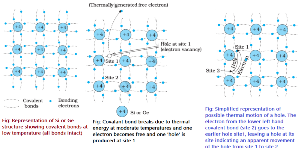
Table of Contents
Extrinsic Semiconductor
When a pure semiconductor is doped with a suitable/desirable impurity, the material obtained is called an extrinsic semiconductor.
- In extrinsic semiconductors, the number of electrons is not equal to the number of holes.
- The electrical conductivity of an extrinsic semiconductor is given by
Electrical conductivity (σ) = 1 / ρ = e (ne μe + nh μh)
ne = electron density μe= mobility of electrons
nh = holes density μh = mobility of holes
e = charge on electrons ρ = resistivity of material
Types of extrinsic semiconductor:
There are two types of extrinsic semiconductor,
- p-type semiconductor
- n-type semiconductor
Important questions based on the Topic
What is an intrinsic semiconductor?
Ans: An intrinsic semiconductor is a pure semiconductor material that has no intentional impurities added to it. It has an equal number of electrons and holes, and its electrical conductivity is determined by the energy gap (bandgap) between the valence and conduction bands.
What is an extrinsic semiconductor?
Ans: An extrinsic semiconductor is a semiconductor material that has been intentionally doped with impurities to alter its electrical properties. Doping creates an excess of either electrons or holes, which increases the material’s electrical conductivity.
What is the difference between an n-type and p-type semiconductor?
Ans: An n-type semiconductor is doped with impurities that provide extra electrons, which become the majority charge carriers in the material. A p-type semiconductor is doped with impurities that create extra holes, which become the majority charge carriers in the material.
How does doping affect the energy band diagram of an extrinsic semiconductor?
Ans: Doping affects the energy band diagram of an extrinsic semiconductor by shifting the position of the Fermi level, which is the energy level where the probability of finding an electron is 50%. This alters the number of free charge carriers in the material and changes its electrical conductivity.
What is the concentration of dopants in an extrinsic semiconductor?
Ans: The concentration of dopants in an extrinsic semiconductor is typically on the order of 10^15 to 10^20 dopant atoms per cubic centimeter of material. This concentration can be controlled during the fabrication process to achieve the desired electrical properties of the material.
What are some common dopants used in extrinsic semiconductors?
Ans: Common dopants used belongs to group III and group V elements,
p-type dopant – Boron
n-type dopants – phosphorus, arsenic, and antimony
How does temperature affect the conductivity of an intrinsic semiconductor?
Ans: The conductivity of an intrinsic semiconductor increases with temperature because higher temperatures provide more energy for electrons to jump from the valence to the conduction band. This creates more free charge carriers and increases the conductivity of the material.
What is the difference between an n-type and p-type semiconductor and an intrinsic semiconductor?
Ans: An n-type or p-type semiconductor is doped with impurities to create an excess of either electrons or holes, while an intrinsic semiconductor has an equal number of electrons and holes. This results in a higher electrical conductivity for doped semiconductors compared to intrinsic semiconductors.
What is the Fermi level of an intrinsic semiconductor?
Ans: The Fermi level of an intrinsic semiconductor is the energy level where the probability of finding an electron is maximum. It is located in the middle of the bandgap and determines the electrical and thermal properties of the material.
What are some applications of intrinsic semiconductors?
Ans: Intrinsic semiconductors are used in a variety of applications, such as in the creation of photovoltaic cells for solar power generation and in the fabrication of high-temperature thermoelectric materials for converting heat into electricity. They are also used as a reference material in the development and calibration of electronic devices.

MY YouTube Channel Link : 👉🖱 https://www.youtube.com/channel/UCGpC7nWE0-bBv9I53MM8qjQ