Table of Contents
Doping
The process of adding desirable impurities to the pure semiconductor is called doping. The impurity atoms added here is called dopants. Doping is done at a ppm level.
After doping semiconductor material obtained is still neutral (have no charge) as dopant atom is added to them not electrons/charge particle and atom as a hole is electrically neutral.
Purpose of doping:
Doping is done to increase the conductivity of semiconductor at desired level and to make conductivity of doped semiconductor almost independent on change in temperature.
Selection of dopants:
The size of dopant atom must be nearly equal to the size of dopant atom so that it does not distort the original pure semiconductor lattice.
| 13 Group | 14 Group | 15 Group |
|---|---|---|
| P type dopant atom | Semiconductor atom | N type dopant atom |
| B 5 | C 6 | N 7 |
| Al 13 | Si 14 | P 15 |
| Ga 31 | Ge 32 | As 33 |
| In 49 | Sn 50 | Sb 51 |
There are two type of dopants used in doping with tetravalent Si or Ge.
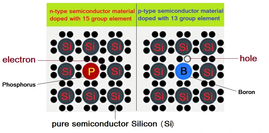
- Pentavalent / Donor impurities (valency 5); like Arsenic (As), Antimony (Sb), Phosphorous (P), etc.
- Trivalent / Accepter impurities (valency 3); like Indium (In), Boron (B), Aluminium (Al), etc.
Methods of doping:
(i) By mixing dopant atom to the pure semiconductor in molten state.
(ii)By heating pure semiconductor in environment of dopant atom
(iii) By bombarding semiconductor with dopant atom.
Important questions from the Topic
What is doping in the context of semiconductors?
Doping in the context of semiconductors refers to the intentional introduction of impurities into a semiconductor material in order to modify its electrical properties.
What types of dopants are commonly used in semiconductor materials, and how do they affect the material’s properties?
Common dopants used in semiconductor materials include boron, phosphorus, arsenic, and antimony belongs to 13th and 15th group elements of periodic table. These dopants can donate or accept electrons, which affects the material’s electrical conductivity, and they can also modify its optical and thermal properties.
How does the doping concentration of a semiconductor material affect its electrical conductivity?
The doping concentration of a semiconductor material can significantly affect its electrical conductivity. Higher doping concentrations generally lead to higher conductivity, since more charge carriers are present in the material.
What is the difference between n-type and p-type doping, and how are they achieved in practice?
N-type and p-type doping refer to the introduction of electrons or holes, respectively, into a semiconductor material. This is achieved by adding dopants that donate or accept electrons, such as phosphorus for n-type doping or boron for p-type doping.
Can a single semiconductor material be doped with both n-type and p-type dopants simultaneously? If so, what is the resulting material called?
Yes, a semiconductor material brick can be doped with both n-type and p-type dopants simultaneously side-by-side. This creates a material known as a semiconductor junction or a p-n junction, which has unique electrical properties that are useful for electronic device applications.
How do the properties of a doped semiconductor material affect the behavior of electronic devices made from it, such as diodes and transistors?
The properties of a doped semiconductor material play a critical role in determining the behavior of electronic devices made from it. For example, the doping concentration can affect the conductivity and resistance of a material, while the type of dopant can affect its optical and thermal properties.
What challenges do researchers and manufacturers face in controlling the doping process in semiconductors, and how are these challenges addressed?
Researchers and manufacturers face a number of challenges in controlling the doping process in semiconductors, including achieving consistent doping concentrations across large wafer substrates, preventing contamination from the doping process, and ensuring the stability of the doped material over time.
What is a conductor, and what does its energy band diagram look like?
Ans: A conductor is a material that has a low resistance to the flow of electrical current. Its energy band diagram shows that the valence and conduction bands overlap, meaning that electrons can move freely throughout the material.
What is a semiconductor, and what does its energy band diagram look like?
Ans: A semiconductor is a material that has an intermediate level of electrical conductivity between a conductor and an insulator. Its energy band diagram shows a small energy gap (bandgap) between the valence and conduction bands. This gap can be overcome by adding energy, such as heat or light, to the material.
What is an insulator, and what does its energy band diagram look like?
Ans: An insulator is a material that has a high resistance to the flow of electrical current. Its energy band diagram shows a large energy gap between the valence and conduction bands, which means that it requires a significant amount of energy to move an electron from the valence band to the conduction band.
What is a rectifier?
A rectifier is an electronic device that converts alternating current (AC) to direct current (DC). It does this by allowing current to flow in only one direction through a circuit, typically using a diode or a series of diodes.
What are the types of rectifiers?
There are two main types of rectifiers: half-wave and full-wave. A half-wave rectifier only allows current to flow in one direction during half of the AC cycle, while a full-wave rectifier allows current to flow in one direction during the entire cycle.
What is reverse breakdown of a junction diode?
Ans: The reverse breakdown of a junction diode is a phenomenon in which a large reverse voltage applied to the diode causes a sudden increase in current flow through the device. This is also known as “reverse breakdown voltage” or “Zener breakdown”.
How does reverse breakdown occur in a junction diode?
Ans: In a junction diode, a depletion region exists between the p-type and n-type semiconductor layers. When a reverse voltage is applied to the diode, the depletion region widens and the electric field across it increases. At a certain voltage, called the breakdown voltage, the electric field becomes strong enough to ionize the atoms in the depletion region and cause a flow of current through the diode.